E-Module Build Guide
 |
Please NoteSome post build modifications were needed after the first build: These instructions need to be updated to reflect the modification that is noted on the electronics check page |
|
|
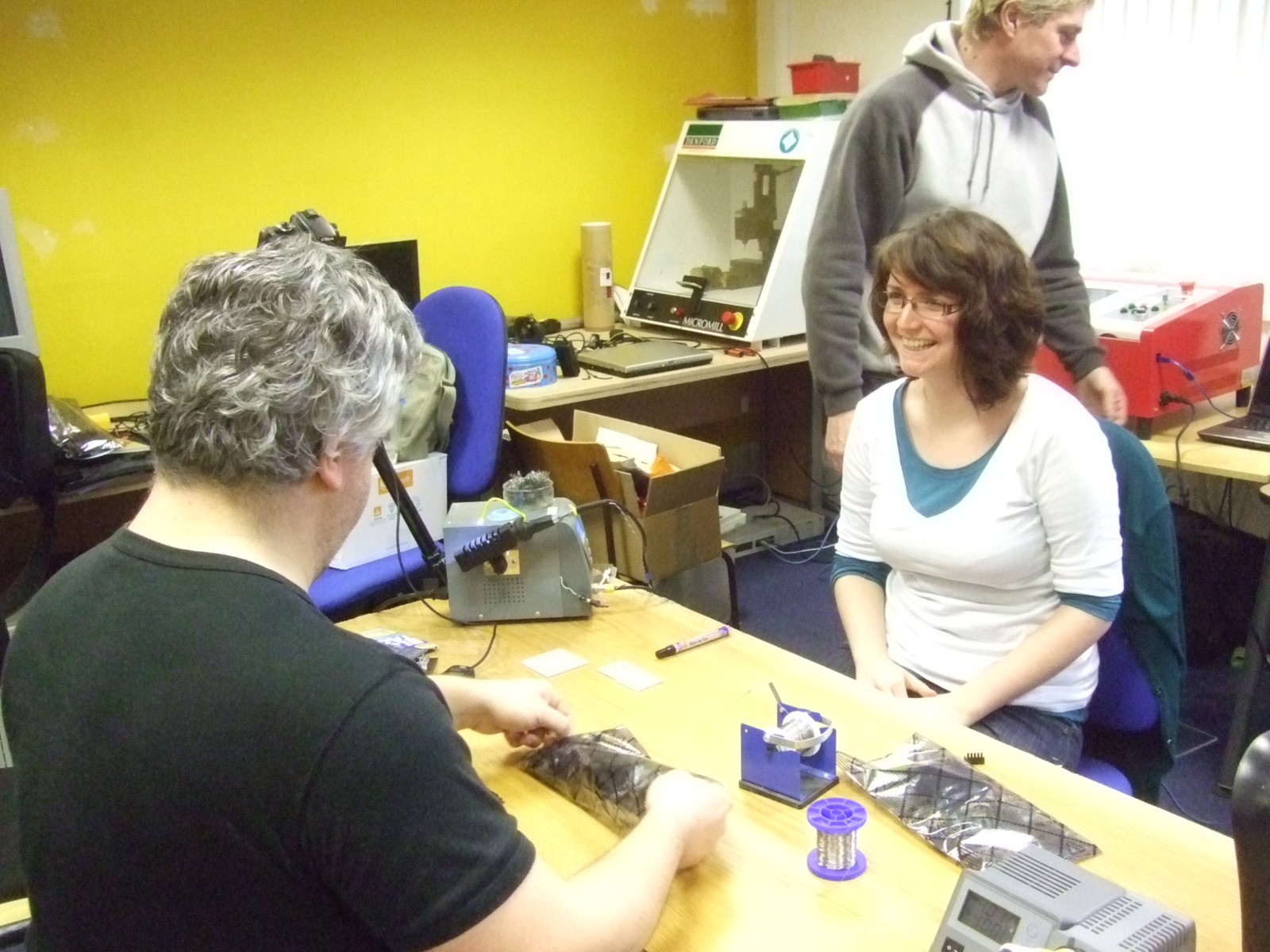
The bag contains some very small items that can easy disappear down holes in the floorboard, eaten by the cat, a child, or be hoovered up etc. Even the brightest and best of our beta testers ended up spilling bits on the floor, so take special care. | |
 |
The black foam parcel contains the chips that are extra sensitive to the "static electricity" that is generated by the artificial fibres in modern clothing in particular. Do not remove the chips from the black foam until you are ready to mount them, and when you do we recommend the use of an anti-static strap or similar precautions. | |
While you're waiting... watch it in real time :) here on YouTube


Pre-assembly checks
- Note: It is possible that some kit parts may vary from this list in look, size and shape. This is where suppliers substituted equivalents. Ask on the forum if you are unsure
- Check parts received are as listed in the BOM (link needed)
- Pay particular note to the capacitors. These are load of blue pills and a few goldy/mustard-coloured ones. They are tricky to read without great eyesight – a magnifier and good lighting will help There should be 3 different values of blue ones. The blue ones are not polarised (ie they do not have a +/- orientation), but the gold coloured ones are.
Lots of blue pills, 2 × 22 pF value for crystal oscillator – 1 for each stepper driver, 4 × 100 pF and lots of 474 pF for decoupling.
- Keep the resistors on their strips as it is easier to sort by value
- Note that the "inductor" looks similar to a large sized resistor
- There are two Surface Mount Components (SMC) resistors in a plastic pouch. These are very tiny and need tweezers to handle easily. They are not static sensitive.
Tools Required
- A clear work area with good lighting, firm smooth surface and comfortable seating
- Soldering iron, if using a variable temperature controlled soldering station, set it to 400°C (or the correct temp for your solder type)
- Steel pan scrubber or other soldering iron tip cleaner
- Thick and fine solder
- Blu-Tack – to hold components while soldering (this tip copyright Michel :) )
- Desolder braid and/or pump – in case of solder bridges
- Long-nose pliers
- Side cutters with flat-back jaws for trimming legs clean to board – the clippings are sharp and fly all over the place unless you cover them with your hand. Beware your eyes
- Tweezers – for placing and holding the surface-mount resistors while soldering
- Anti static earthing strap
- An LED torch or other bright light source for – reading capacitor values
- Magnifier
- Resistor colour code chart and/or multimeter for identifying resistors
- A "Do Not Disturb" Sign
Board note

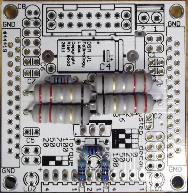
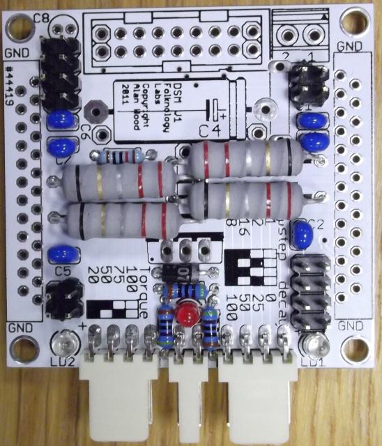
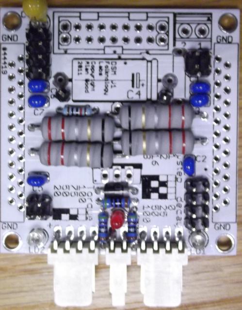
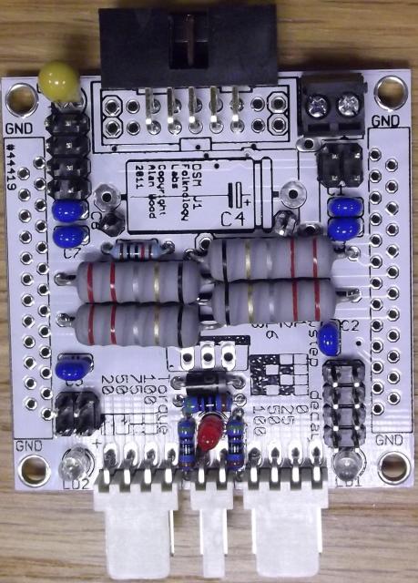
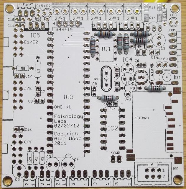
You have two smaller square boards that are the two twin driver module boards. We will build these first. Each step is applied to each board in turn. Each board has two sets of components – one for each driver circuit. However this board is no longer two exactly mirrored halves as it was in earlier designs that Al showed us.
For the purpose of these instructions the board is oriented so the writing is the correct way up and C8 is marked in the top left hand corner
2 x Driver Boards |
|
|---|---|
Step 1 – Resistors |
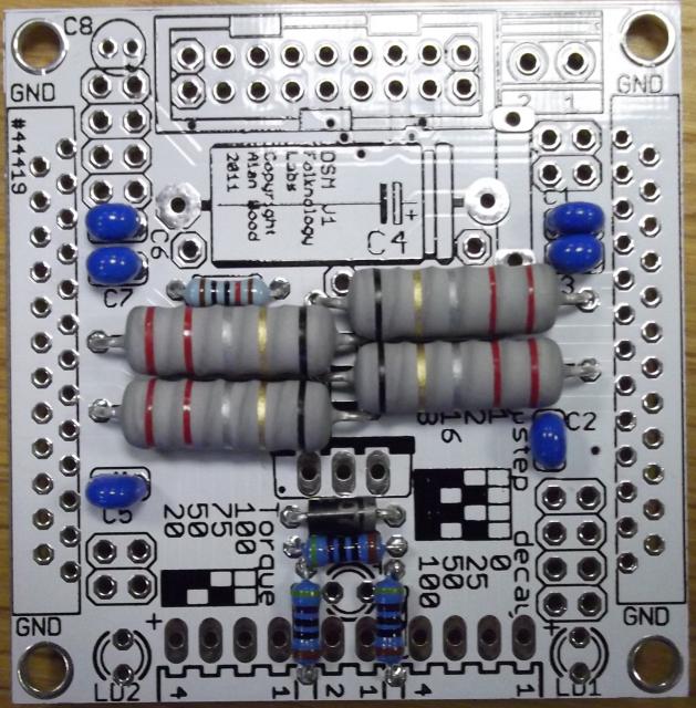
Fit three resistors of 470 Ω at R3, R6, and R8 (yellow/violet/black/black/brown) [these are the LED resistors] – Resistors are not polarised components. Fit one resistor of 10 kΩ at R7 (brown/black/black/red/brown) [this is the MOSFET base resistor] |
 
|
Step 2 |
|
|
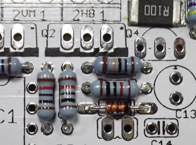
Fit the four large (220 mΩ) resistors at R1, R2, R4 and R5 (red/red/silver/gold/black). Check that you use the correct holes, as there is a test point hole close to the R2 left leg position. |
|
Step 3 – Blue capacitors |
|
|
Fit two blue 100 pF capacitors (marked "101") at C1 and C5 [these are to set the chopper frequency on the steppers]. The markings for C1 could cause confusion – refer to the picture for correct placement. Check the values carefully: there are 3 different values, 22, 101 and 474, all in similar packages. The value is marked in tiny writing on the component. These are not polarised components. |

|
Step 4 |
|
|
Fit four blue 470 nF capacitors (marked "474") at C2, C3, C6 and C7 [decoupling caps]. |
|
Step 5 |
|
|
Fit the black diode in the centre bottom of the board above the trio of resistors. [Protection diode for MOSFET].
|
|
Step 6 – LEDs |
|
|
Fit the two LEDs with clear lenses (which shine orange) to LD1 and LD2 at the bottom of the board.
You can confirm this using the diode or LED setting on a multimeter (if you have access to such an up-market meter) or by using a resistor and a power source. (more info needed about how to do this) Fit one red-cased LED in the centre of the trio of resistors at the bottom of the board, remembering that + is the long leg and goes into the right-hand hole. The marking on the board is partially hidden at this point by the resistor. |
|
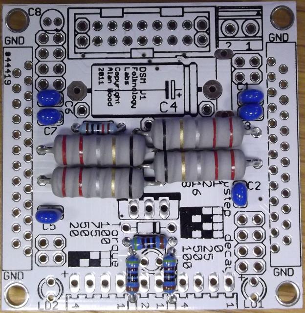
Step 7 |
|
|
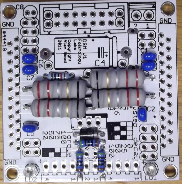
Fit three connectors at the bottom of the board, the 2-pin connector in the centre, and the two 4-pin connectors to left and right [one for each stepper motor]. Take care that they stay aligned flat to the board as you solder them in. The Blu-Tack tip is particularly helpful here.
|

|
Step 8 |
|
|
Optional step: here we fit two test pins either side of the C4 capacitor marking. These are used to provide a place to get a trigger signal for an oscilloscope when testing the chopper decay. There is a place for a third pin as GND, but is is very close to the large resistor and so is not being fitted. There are many alternative GND points on the board that are easier to connect to anyway. These single pins can be very fiddly to solder, so the choice is yours. In further pictures they are not shown. |

|
Step 9 |
|
|
Fit the two 8-pin headers, JP1 and JP2. [for jumpers to set decay & step sizes] These are not handed, and can go either way around, so long as the long pins face up from the board.
|
|
Step 10 |
|
|
Fit the two 4-pin headers JP3 and JP4. They are not handed and can go either way around, so long as the long pins face up from the board. Make sure these headers are mounted flush to the board so they don't lean. As above, be careful with overheating. |
|
Step 11 |
|
|
After those two simple steps, this one needs more concentration.
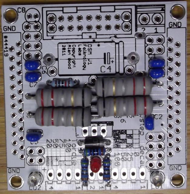
Fit gold coloured tantalum capacitor 47 μF at top left C8.
|
|
Step 12 |
|
|
Fit right angled black boxed header [link to controller board] Note: the design allows for a wider 14-pin connector with extended functionality. The TVRR reference build uses a narrower 10-pin header that fits in the centre of the hole array. Tack the corners first and ensure each pin has a good amount of solder applied to anchor the header to the board. |

|
Step 13 |
|
|
Fit the 2-pin screw terminal block. |
|
Step 14 |
|
|
Fit the large black 220 μF electrolytic capacitor at C4.
|

|
Step 15 |
|
|
|
  
|
Step 16 |
|
|
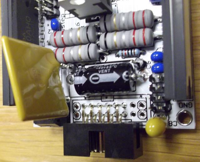
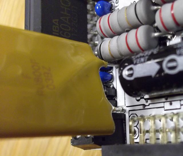
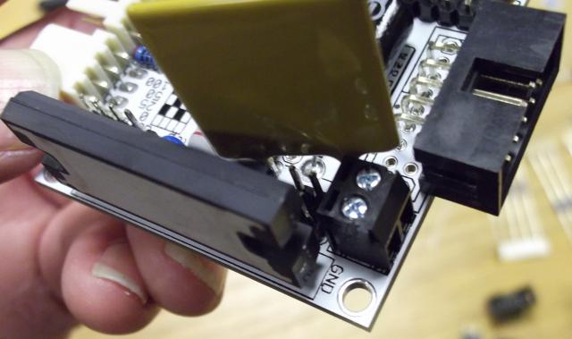
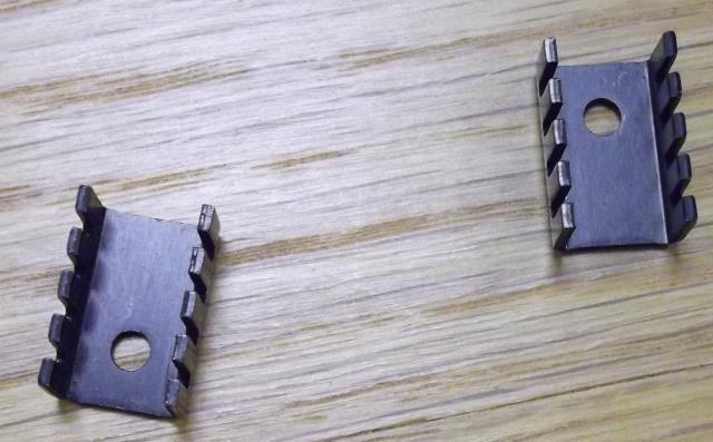
Note: It is best to protect the MOSFET from static charges. In the pic we see a professional system, but touching an earthed pipe or metal PC case is an alternative. If your board is looking like this reverse side then it is "lookin' good". |
|
Step 17 |
|
|
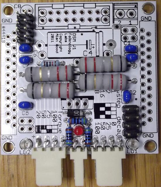
Fitting the last item on these boards, the PTC (solid state resettable fuse). This is a large and incongruous component that has given Al more grief that most of the others! It is a little tricky as the space is tight and the legs need to be 'adjusted' to fit around the adjacent components so they are not touching one anywhere, while being careful not to crack the PTC itself. Using some pointed pliers to protect the top of the leg during bending is a handy tip. |
|
Step 18 |
|
|
Now you should fit the jumpers to the places as shown in this photo. Please note that the board markings are inaccurate for the 1st Build Group, and you should instead trust this photo. |
|
 This component is polarised and must be fitted with the silver band to the right, aligning with the black strip in the board markings.
 Static care: Now to fit the most important components! The two stepper drivers are large and, like a millipede, have many legs. Hopefully yours are all in line and straight. If not, now is the time to align them. Apart from the number of legs, they should be straightforward to fit. Clean joints and the right amount of solder is important. Too much solder may cause shorts on either side of the board; not enough may cause 'dry joints' after extended use. They are not difficult to fit – just check the joints with a magnifier, and they are good chunky things to fit!
Time for Pizza – Two boards down and one to go!
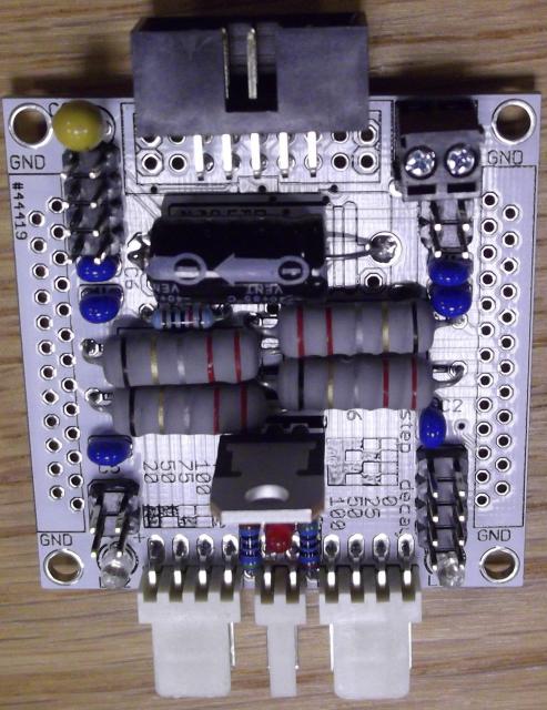
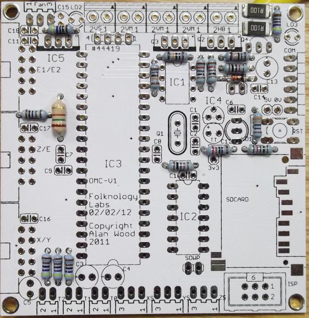
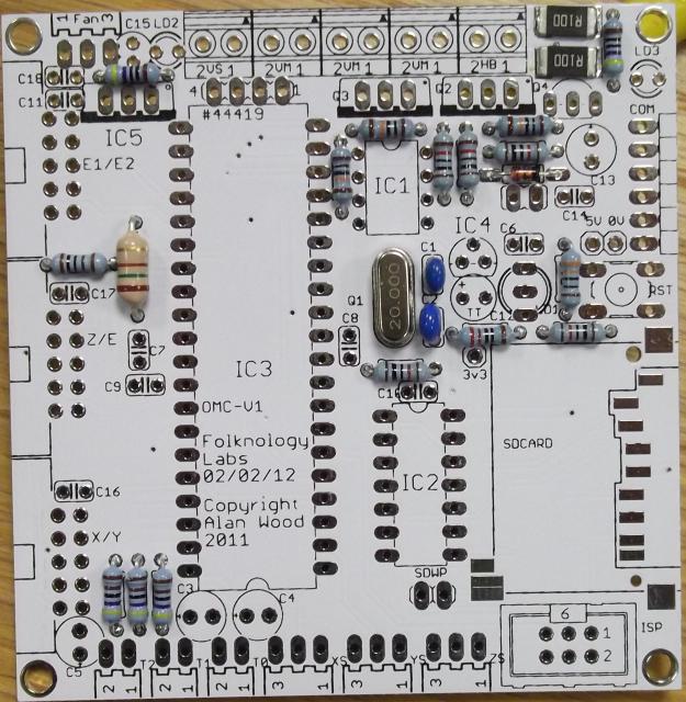
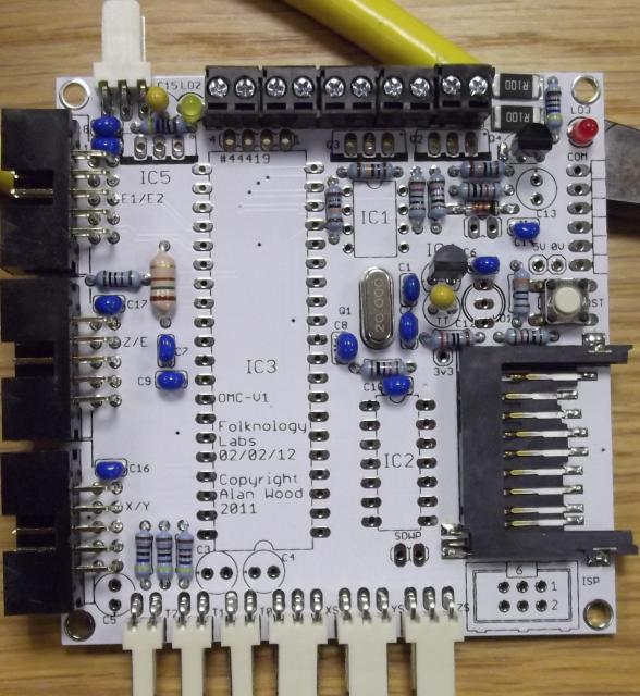
1 × Controller BoardThese steps do not cover soldering in the Optional Test Pins at 0 V, 3.3 V and 5 V positions marked on board | |
|---|---|
Step 1 |
|
|
Fit 10 kΩ (brown, black, black, red, brown) resistors at R1 (Note: this is incorrectly marked R11 – a through-hole – on the board, refer to pic), R5, R6, and R17. Leave the resistors raised a little above the board, this will allow you to 'ease' their position if needed when fitting adjacent components later.
|

|
Step 2 |
|
|
Fit three 100 kΩ (brown, black, black, orange, brown) resistors at R7, R12, and R20. Leave R20 a little raised above the board, you need to ensure the DIL Sockets to left and right of R20 can be mounted in a later step, and R20 may need to be 'eased' |
|
Step 3 |
|
|
Fit three 4.7 kΩ (4K7 yellow, violet, black, brown, brown) resistors at R2, R3, R4 at the bottom left of the board. |
|
Step 4 |
|
|
Fit a 220 Ω (red, red, black, black, brown) resistor at R9, above the SD card marking. Fit a 330 Ω (orange, orange, black, black,brown) resistor at R10, above and to the right of R9. Fit a 1 kΩ (brown, black, black, brown, brown) resistor at R8, on the left-hand side, a little above halfway up the board. |

|
Step 5 |
|
|
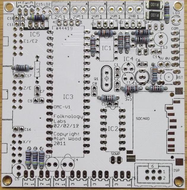
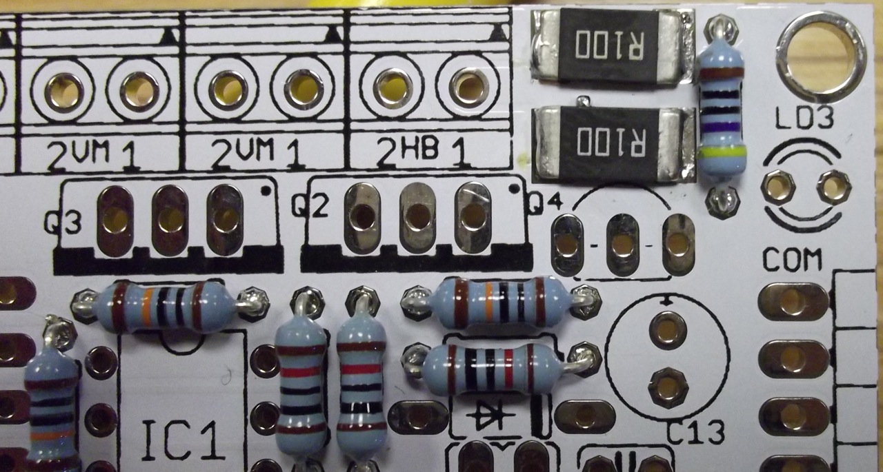
Fit two 50 mΩ surface mount resistors (marked "R050") at R11 and R14 in the top right corner (there are, in fact, two resistor places marked R11 on the board, but the other is for the through-hole component that we fitted in step 1).
There is a knack to fitting these: Put a small amount of solder on one of the two pads. Use tweezers to place the resistor (either way around, depending on your own handedness) and heat the soldered pad to fix the component. Finally, solder the other end.
|

|
Step 6 |
|
|
Fit two 470 Ω resistors at R15, on the top right of the board by the surface mounts, and at R16, on the top left of the board. Note - it is recommended to fit R15 on the bottom of the board (not as shown in the picture) to keep it away from the heat sink that will be attached to the 2 SMD resistors (R11 & R14) |
|
Step 7 |
|
|
There is no Step 7. (this step is left intentionally blank :) ) |
|
Step 8 |
|
|
Fit the diode – a small orange-coloured component.
|
|
Step 9 |
|
|
Fit the beige inductor (brown/green/brown/gold – 150 μH) in L1 on the left side of the board, a little over halfway up. It is not polarised. |
|
Step 10 |
|
|
Fit two blue 22 pF capacitors at C1 and C2, to the right of the crystal. Double check that you have the 22 pF ones. They are not polarised. Fit the 20 MHz Crystal. Leave this raised a small amount above the board, as the case of the crystal should not touch any of the tracks or components near it. You may wish to use a small piece of thin cardboard as a spacer while you solder it. It is not polarised. |
|
Step 11 |
|
|
Fit the rest of the 470 pF blue capacitors (10 in all, marked "474") at C6, C7, C8, C9, C10, C11, C14, C16, C17 and C18. These are not polarised. |
|
Step 12 |
|
|
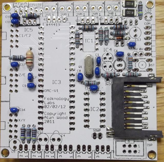
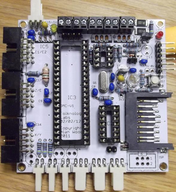
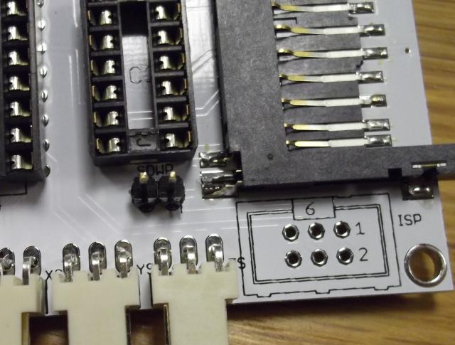
Fit the SD Card holder. It has bumps on its underside that should hold it in position through the two holes near the edge of the board. It should bump into position exactly; solder the two outside tabs first and then the inner and outer legs. All soldering is on the top for this surface-mount component. UPDATE:18May2012: There has been questions on the GG about the 3 pins at the rear of the SD card socket (bottom right in pic), if you refer to the previous pic you will there are 3 pads, 2 of which are very close together. It is best to keep from bridging the pads with solder, though if you do so it will *NOT* cause any problems because the current firmware does not use the signals on these pins which are for the SD card detect 'write protect' function |
|
Step 13 |
|
|
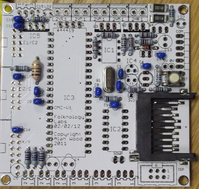
Fit the reset button. The legs extend out to the left and right, but the button can be placed either way around. |
|
Step 14 |
|
|
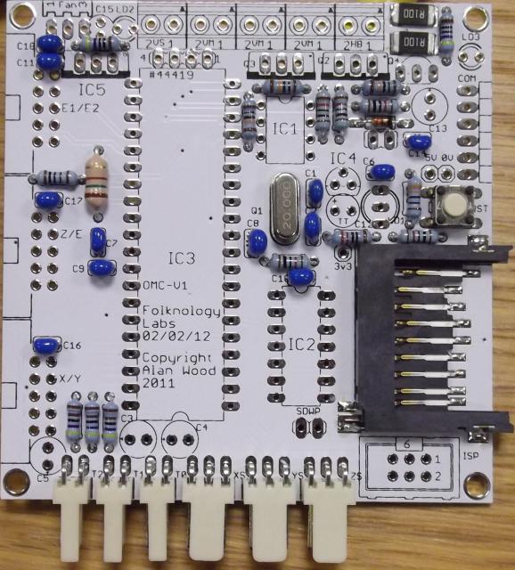
Fit three 2-pin connectors and three 3-pin ones at the bottom of the board. [thermistor (2-pin) and endstop (3-pin) connectors] |
|
Step 15 |
|
|
Fit one 3-pin (fan) connector to the top left of the board. |

|
Step 16 |
|
|
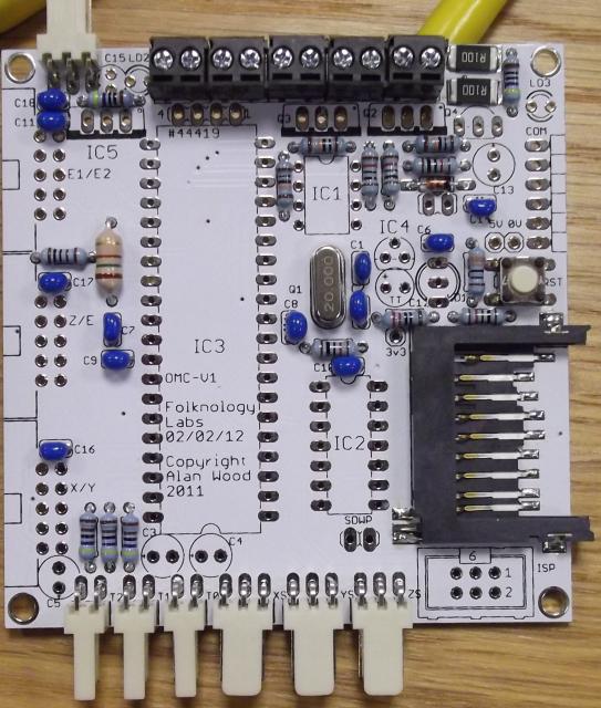
Fit the five dual screw terminals at the top of the board. Facing outward. |
|
Step 17 |
|
|
Fit the right-angled black-boxed 10-pin headers on the left side of the board [connections for cables to driver modules]. |

|
Step 18 |
|
|
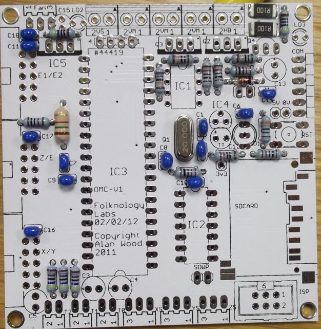
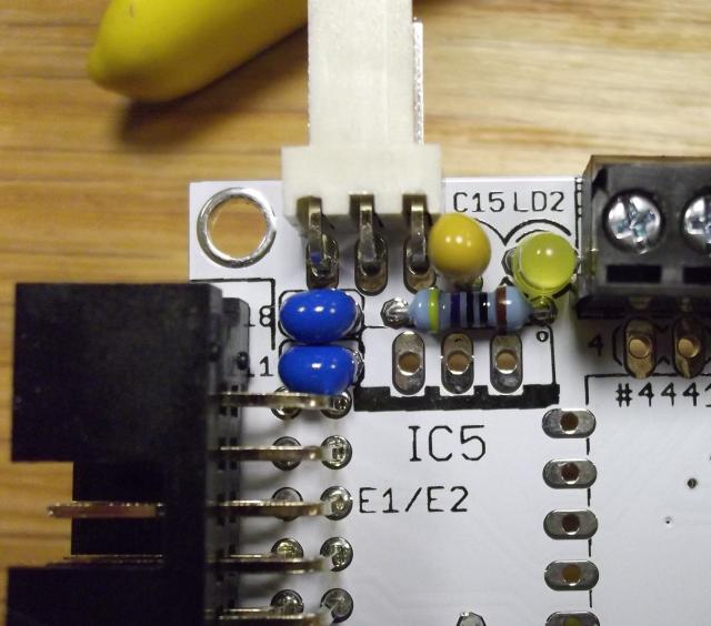
Fit the yellow LED at LD2 with its long lead (anode, +) to the left and shorter lead (cathode, GND, -) closest to the screw terminals on the right. Fit the smaller gold-coloured tantalum 1 μF capacitor at the top left in the position marked C15.
|
|
Step 19 |
|
|
Fit the red LED at LD3 with its long lead (positive, +) on the left, towards the centre of the board, and the short lead (GND, -) on the side nearer the edge of the board. Fit the transistor labelled BC559 at Q4 with the flat face towards the bottom of the board, as per the markings on the board. Don't confuse this with the part for IC4 that is in the same type of package. |

|
Step 20 |
|
|
Fit the larger gold-coloured tantalum 5.8 μF (or maybe 6.8 μF) capacitor at C12 below IC4.
|
|
Step 21 |
|
|
Fit the tri-colour LED at LD1. The longer of the outer legs (red light) goes at the bottom, toward R9. If this is the wrong way round the RGB lamps will light incorrectly. |

|
Step 22 |
|
|
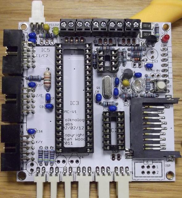
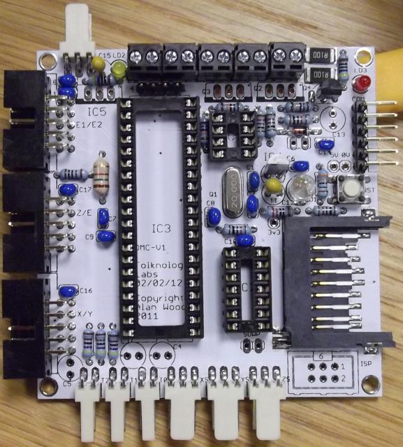
Fit the three DIL IC sockets. Your sockets may be marked with a notch or a square hole that aligns with the marking on the board, i.e. at the bottom for the large IC1 and at the top for the two small ones at IC2 and IC3. Check closely before soldering to ensure all legs are protruding evenly through the holes on the back of the board. It is easy to have one fold under the socket while fitting all the legs through. Tack the diagonal corner pins and check the socket is flat against the board before soldering the rest of the legs. Be quick, to avoid overheating any single pin, which risks melting the plastic socket. |
|
Step 23 |
|
|
Fit the 4-pin header at the top of the IC3 socket. Fit the right-angle 6-pin connector at the top right below the red LED – take care with heating and alignment as before. Fit the one 2-pin jumper in the space marked SDWP at the bottom of the board, and a second below the diode and above C6 on the top right. (SDWP stands for SD card Write Protect.) |
|
Step 24 |
|
|
Fit the SPI/ISP header at the bottom right. The ISP header is polarised, so follow the shape marked on the board to ensure correct orientation. The slot in the side should be towards the SD card. Fit the four 10 μF electrolytic capacitors (black cans) at C3, C4, C5, C13.
|
|
Step 25 |
|
|
Fit the voltage regulator 7805 at IC5, and the two MOSFETs marked 4P03L04 at Q2 and Q3, orientated so that the metal heatsink back faces down toward the centre of the board. This side is marked with a black bar on the board. It was originally envisaged that extra external separated heatsinks would be required for the MOSFETs, but experience has shown that the external heatsinks are not generally required - the MOSFETs have behaved themselves well under load. |
|
Testing |
|
|
|
|
Step 26 |
|
|
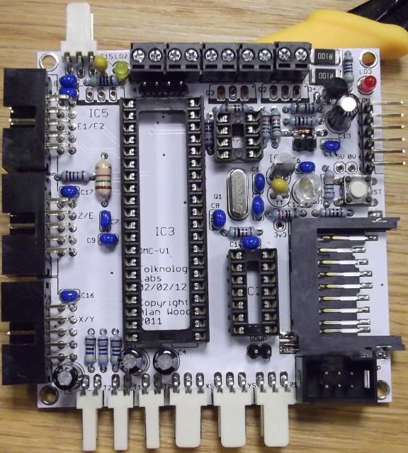
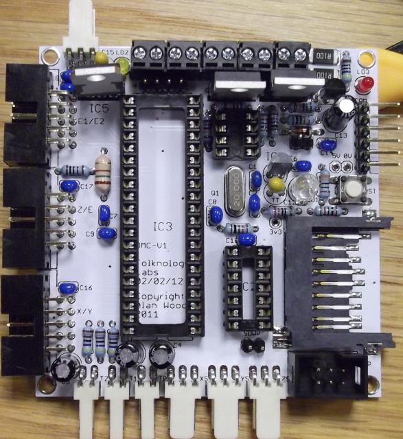
Fit the chips, observing correct orientation. The legs of DIL chips may need 'easing' inward by pressing each row of pins on a firm, flat, non-static surface. You can use the anti-static bag as a mat to do this. |
|
YAY!
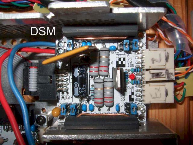
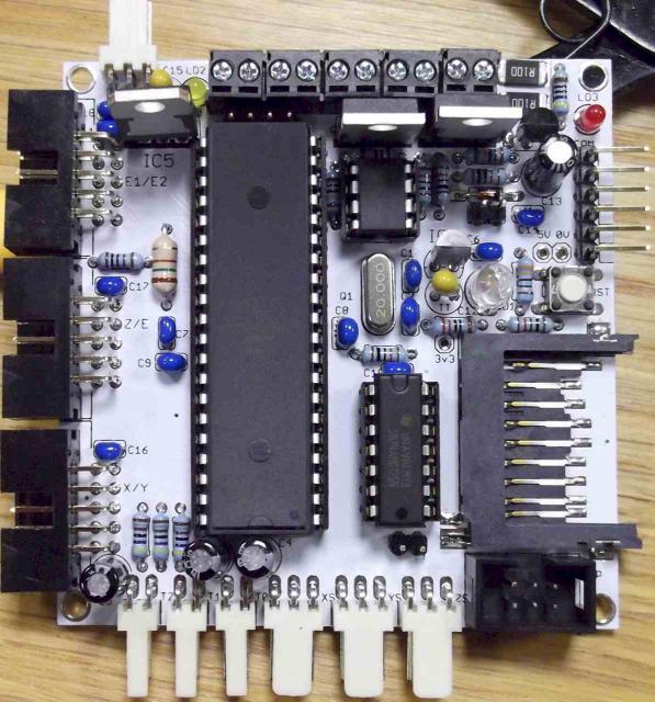
Mounted boards
Here is a view of the prototype V1 boards (with some significant differences that you can spot) mounted on the TVRR beta machine for testing. They are shown here to give an idea of how the boards might be mounted and wired. You can also see additional heat-sinks (8 sets of splayed aluminium fins) that have been added to the stepper drivers.
