E-Module-Build-OMC-v1.2
 |
If you find any discrepancies, let someone know or change it |
|
|
The box contains some very small items that can easy disappear down holes in the floorboard, eaten by the cat, a child, or be hoovered up etc. Even the brightest and best of our beta testers ended up spilling bits on the floor, so take special care. | |
 |
The black parcel contains the chips that are extra sensitive to the "static electricity" that is generated by the artificial fibres in modern clothing in particular. Do not remove the chips from the black foam until you are ready to mount them, and when you do we recommend the use of an anti-static strap or similar precautions. | |


Pre-assembly checks
- Note: It is possible that some kit parts may vary from this list in look, size and shape. This is where suppliers substituted equivalents. Ask on the forum if you are unsure
- Check parts received are as listed in the BOM
- Pay particular note to the capacitors. These are load of blue pills and a few goldy/mustard-coloured ones. They are tricky to read without great eyesight – a magnifier and good lighting will help. There should be 3 different values of blue ones. The blue ones are not polarised (ie they do not have a +/- orientation), but the gold coloured ones are.
- Keep the resistors on their strips as it is easier to sort by value
- Note that the "inductor" looks similar to a large sized resistor
Tools Required
- A clear work area with good lighting, firm smooth surface and comfortable seating
- Soldering iron, if using a variable temperature controlled soldering station, set it to 365°C (or the correct temp for your solder type)
- Steel pan scrubber or other soldering iron tip cleaner
- Thick and fine solder
- Blu-Tack – to hold components while soldering (this tip copyright Michel :) )
- Desolder braid and/or pump – in case of solder bridges
- Long-nose pliers
- Side cutters with flat-back jaws for trimming legs clean to board – the clippings are sharp and fly all over the place unless you cover them with your hand. Beware your eyes
- Tweezers – for placing and holding the surface-mount resistors while soldering
- Anti static earthing strap
- An LED torch or other bright light source for – reading capacitor values
- Magnifier
- Resistor colour code chart and/or multimeter for identifying resistors
- A "Do Not Disturb" Sign
Board note

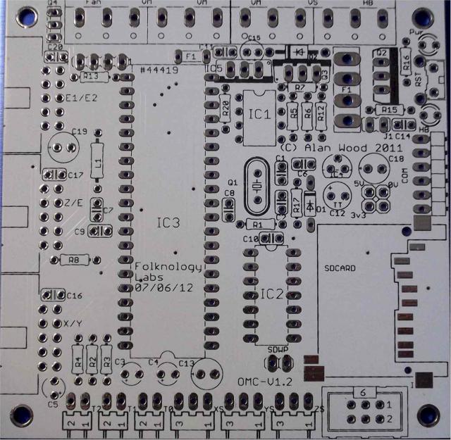
You have two smaller square boards that are the two twin driver module boards. We will build these first. Each step is applied to each board in turn. Each board has two sets of components – one for each driver circuit. However this board is no longer two exactly mirrored halves as it was in earlier designs that Al showed us.
For the purpose of these instructions the board is oriented so the writing is the correct way up and C8 is marked in the top left hand corner
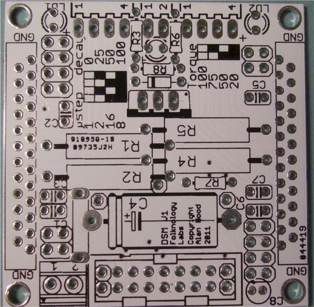
2 x Driver Boards |
|
|---|---|
Step 1 – Resistors |
|
|
Fit three resistors of 470 Ω at R3, R6, and R8 (yellow/violet/black/black/brown). For Round 3 these may be 510Ω (green,brown,black,black,brown). [these are the LED resistors] – Resistors are not polarised components. |
|
Step 2 |
|
|
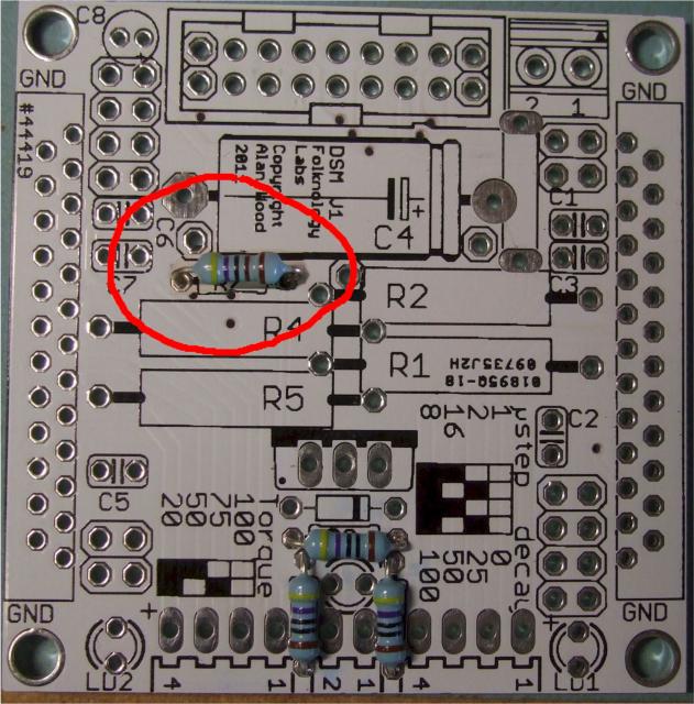
Fit one resistor of 4.7kΩ at R7 (yellow/violet/black/brown/brown) [this is the MOSFET base resistor] |
|
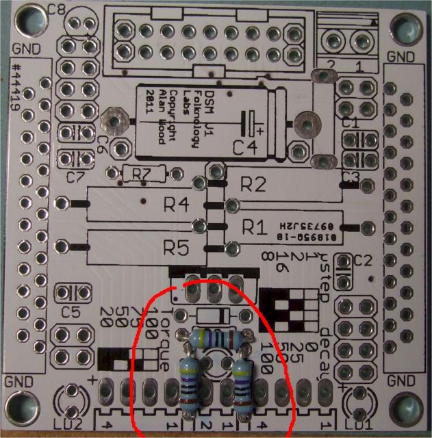
Step 3 – Large Resistors |
|
|
Fit the four large (220 mΩ) resistors at R1, R2, R4 and R5 (red/red/silver/gold/black with a green background). Check that you use the correct holes, as there is a test point hole close to the R2 left leg position. |
|
Step 4 – Small capacitors |
|
|
Fit two brown (tan) 100 pF capacitors (marked "101") at C1 and C5 [these are to set the chopper frequency on the steppers]. The markings for C1 could cause confusion – refer to the picture for correct placement. Check the values carefully: there are 3 different small capacitor values, 22, 101 and 474, all in similar packages. The value is marked in tiny writing on the component. These are not polarised components. |

|
Step 5 |
|
|
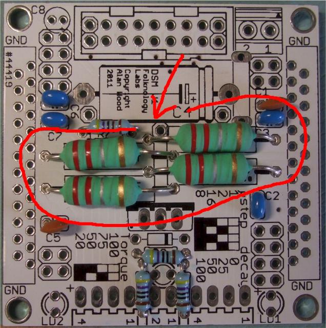
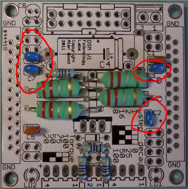
Fit four blue 100nf capacitors marked "104" (some of these may instead be marked as "474" but can be used interchangeably) at C2, C3, C6 and C7 [decoupling caps]. |
|
Step 6 |
|
|
Fit the black diode in the centre bottom of the board above the trio of resistors. [Protection diode for MOSFET].
|
|
Step 7 – LEDs |
|
|
Fit the two square yellow cased LEDs to LD1 and LD2 at the bottom of the board. Make sure these are upright and leave maximum room for fitting the adjacent 8 pin header later
You can confirm this using the diode or LED setting on a multimeter (if you have access to such an up-market meter) or by using a resistor and a power source. (more info needed about how to do this) |
 |
Step 8 |
|
|
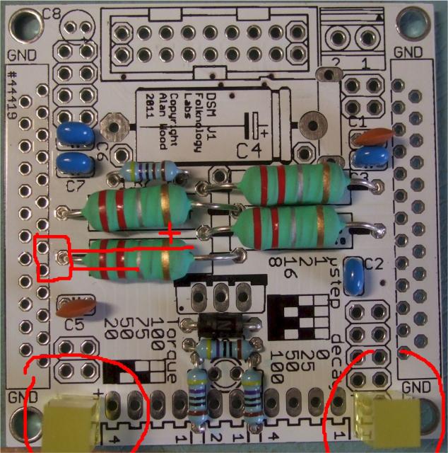
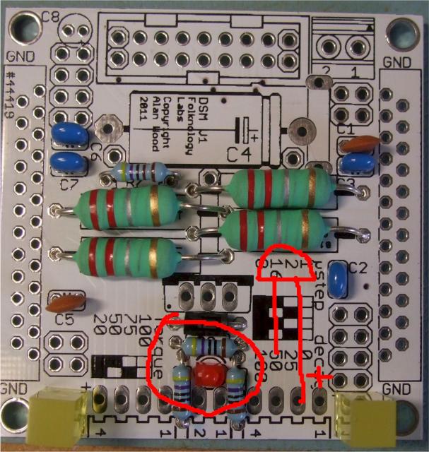
Fit one red-cased LED (small red rectangle with a dome) in the centre of the trio of resistors at the bottom of the board, remembering that + is the long leg and goes into the right-hand hole. The marking on the board is partially hidden at this point by the resistor
|
|
Step 9 |
|
|
Fit three connectors at the bottom of the board, the 2-pin connector in the centre, and the two 4-pin connectors to left and right [one for each stepper motor]. Take care that they stay aligned flat to the board as you solder them in. The Blu-Tack tip is particularly helpful here.
|

|
Step 10 ‐ Skip This Step |
|
|
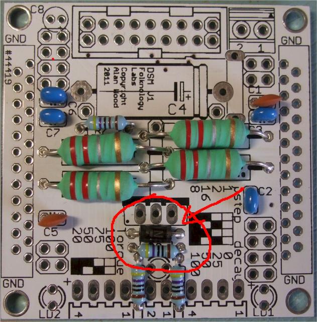
Optional step - not recommended, can be added later if needed: here we can fit two test pins either side of the C4 capacitor marking. These are used to provide a place to get a trigger signal for an oscilloscope when testing the chopper decay. There is a place for a third pin as GND, but is is very close to the large resistor and so is not being fitted. There are many alternative GND points on the board that are easier to connect to anyway. These single pins can be very fiddly to solder, so the choice is yours. In further pictures they are not shown, and this pic is from v1.0 and provided for reference to the pin position only |

|
Step 11 |
|
|
Fit the two 8-pin headers, JP1 and JP2. [for jumpers to set decay & step sizes] These are not handed, and can go either way around, so long as the long pins face up from the board.
Note that these headers may have been created by chopping off from a longer length, so the ends may not be very square and neat. In particular one of the headers is rather close to the yellow LED 1, so consider whether you need to file or cut your header to trim it so it fits ok. |
|
Step 12 |
|
|
Fit the two 4-pin headers JP3 and JP4. They are not handed and can go either way around, so long as the long pins face up from the board. Make sure these headers are mounted flush to the board so they don't lean. As above, be careful with overheating. |

|
Step 13 |
|
|
After those two simple steps, this one needs more concentration.
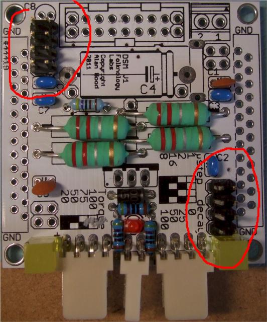
Fit gold coloured tantalum capacitor 22μF at top left C8. For Round 3 boards these may be 33μF
|

|
Step 14 |
|
|
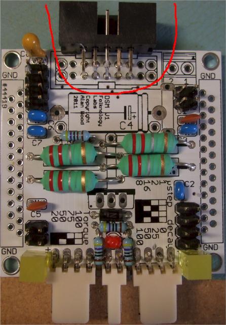
Fit right angled black boxed header [link to controller board] Note: the design allows for a wider 14-pin connector with extended functionality. The TVRR reference build uses a narrower 10-pin header that fits in the centre of the hole array. Tack the corners first and ensure each pin has a good amount of solder applied to anchor the header to the board. |
|
Step 15 |
|
|
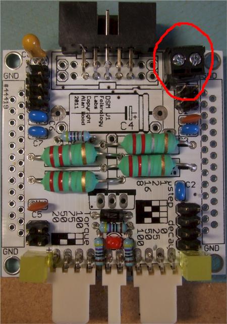
Fit the 2-pin screw terminal block facing up/outward. It will take extra solder to make a strong joint. This component will be subject to mechanical stress when in use |
|
Step 16 |
|
|
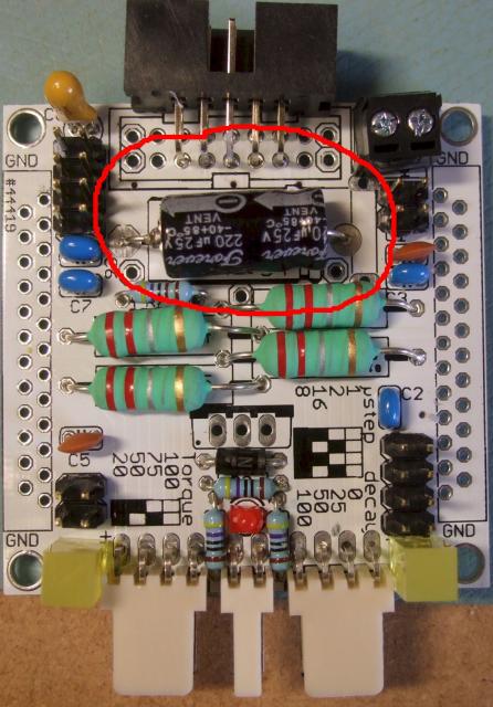
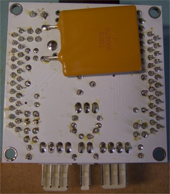
Fit the large black 220 μF electrolytic capacitor at C4.
|
|
Step 17 |
|
|
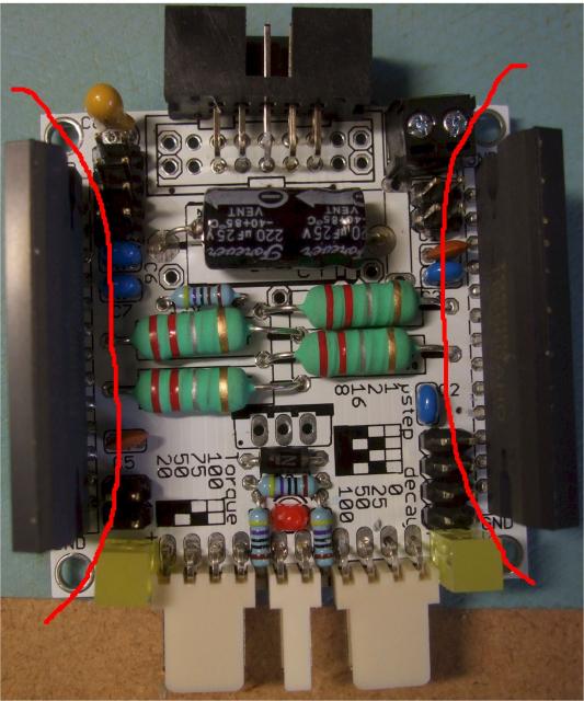
Apart from the number of legs, they should be straightforward to fit. Ensure they a vertical, this is important for mounting to a heatsink later. Making good joints and the using the right amount of solder is important. Too much solder may cause shorts on either side of the board; not enough may cause 'dry joints' after extended use. They are not difficult to fit – just check the joints with a magnifier on both sides of the joints. |
|
Step 18 |
|
|
Note: It is best to protect the MOSFET from static charges. In the pic we see a professional system, but touching an earthed pipe or metal PC case is an alternative. |
|
Step 19 |
|
|
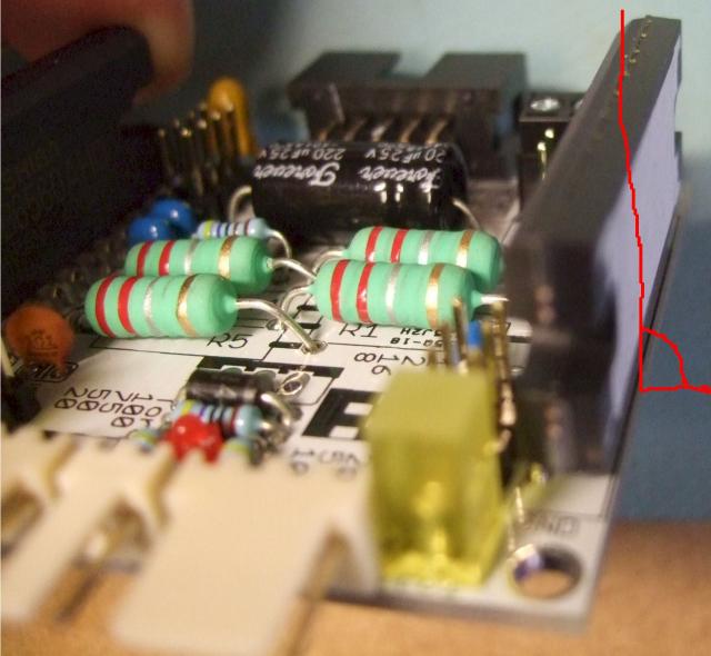
Fitting the last item on these boards, the PTC (solid state resettable fuse). This is a large and incongruous component that has given Al more grief that most of the others! It was a little tricky and ugly when previously mounted on the top of the board, thanks to Barnaby for suggesting that we fit underneath. The legs need to be bent to 90 degrees while being careful not to crack the PTC itself. Using some pointed pliers to protect the top of the leg during bending is a handy tip. Looking at the underside of the board, if the previous steps are all correct, there should be only two holes available in the top left, this component is not polarised. Do a test placement, check the legs protruding into the top side of the board, remove and then trim the legs of surplus length before soldering in place. One leg will be need to be trimmed shorter than the other. The pic also shows the underside of the board before cleaning the flux off the board. If you look closely at the full sized pic, you can see why examining the board closely with a magnifier will pay dividends later :) |
|
Step 20 |
|
|
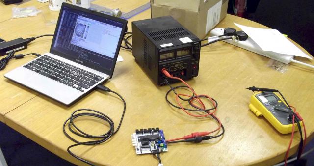
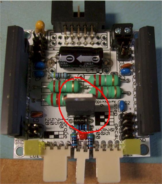
At this stage you should do the electrical check on the boards, before adding the jumpers. Fit the jumpers to the places as shown in this photo. Please note that the board markings are inaccurate (as for the 1st Build Group) and you should, instead, trust this photo for jumper positioning. |
|
 This component is polarised and must be fitted with the silver band to the right, aligning with the black strip in the board markings.
 Static care: Now to fit the most important components! The two stepper drivers are large and, like a millipede, have many legs. Hopefully yours are all in line and straight. If not, now is the time to align the legs.
Time for Pizza – Two boards down and one to go!
1 × Controller Board - for Version 1.2 Only
| |
|---|---|
Step 1 |
|
|
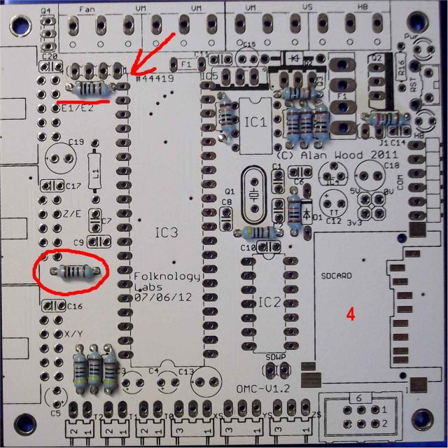
Fit four 4.7kΩ (4K7 yellow, violet, black, brown, brown) resistors at R1,R2, R3, R4. Leave the resistors raised a little above the board, this will allow you to 'ease' their position if needed when fitting adjacent components later. |
|
Step 2 |
|
|
Fit 10kΩ (brown, black, black, red, brown) resistors at R5, R6, and R17. Leave the resistors raised a little above the board, this will allow you to 'ease' their position if needed when fitting adjacent components later. |
|
Step 3 |
|
|
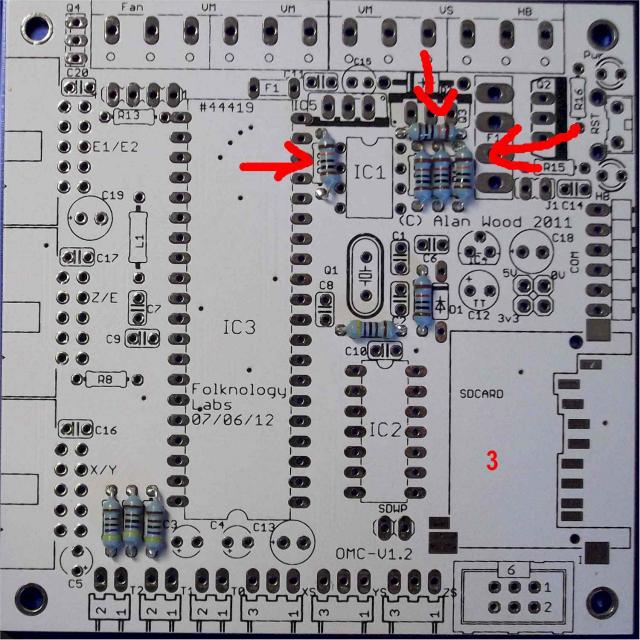
Fit three 100 kΩ (brown, black, black, orange, brown) resistors at R7, R12, and R20. Leave R20 a little raised above the board, you need to ensure the DIL Sockets to left and right of R20 can be mounted in a later step, and R20 may need to be 'eased' |
|
Step 4 |
|
|
Fit the 1 kΩ (brown, black, black, brown, brown) resistors at R8, on the left-hand side, a little above halfway up the board and R13.
Alternatively, before fitting R13, take part of step 24 out of order and fit the 40 pin socket. Tack the socket in place by soldering the (viewed from above) top right and bottom left pins (do pay attention to step 24's warning about ensuring all the pins of this socket are straight). That way, when fitting R13, you can solder both R13 and the adjacent pin of the socket. |
|
Step 5 |
|
|
Fit a 220 Ω (red, red, black, black, brown) resistor at R15. Leave the resistors raised a little above the board, this will allow you to 'ease' their position if needed when fitting adjacent components later. |
|
Step 6 |
|
|
Fit 470Ω (yellow,purple,black,black,brown) at R16 on the top right of the board. For Round 3 these may be 510Ω (green,brown,black,black,brown). |

|
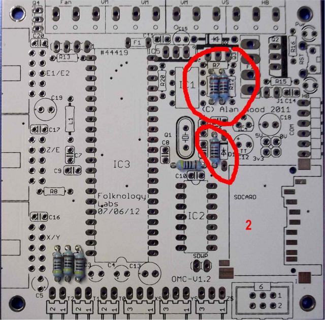
Step 7 |
|
|
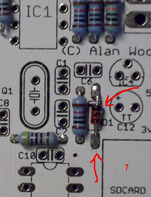
Fit the diode – a small orange-coloured component at D1.
|
|
Step 8 |
|
|
Fit black diode at D2.
|
|
Step 9 |
|
|
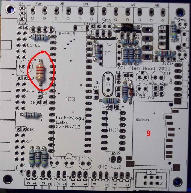
Fit the beige inductor (red/red/brown/gold – 220 μH) in L1 on the left side of the board, a little over halfway up. It is not polarised. |
|
Step 10 |
|
|
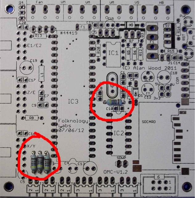
Fit tiny two honey coloured 22 pF capacitors at C1 and C2, to the right of the crystal position. Double check that you have the 22 pF ones. They are not polarised. NOTE (admg 2014-02-09): For Round 3 these are the same value but round, tan coloured capacitors. |
|
Step 11 |
|
|
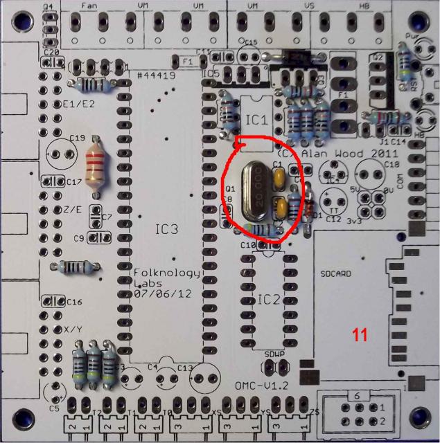
Fit the 20 MHz Crystal. Leave this raised a small amount above the board, as the case of the crystal should not touch any of the tracks or components near it. You may wish to use a small piece of thin cardboard as a spacer while you solder it. It is not polarised. |
|
Step 12 |
|
|
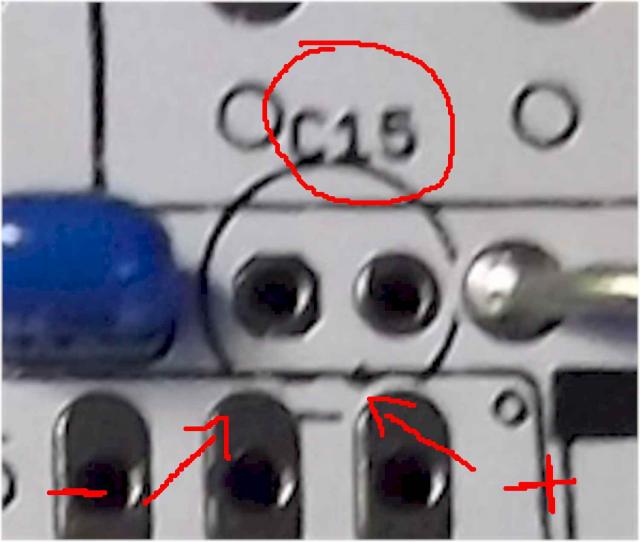
Fit the rest of the 100nf (and/or 470nf if you have those instead) blue capacitors (10 in all, marked "104" or "474") at C6, C7, C8, C9, C10, C11, C14, C16, C17 and C20. These are not polarised. |

|
Step 13 |
|
|
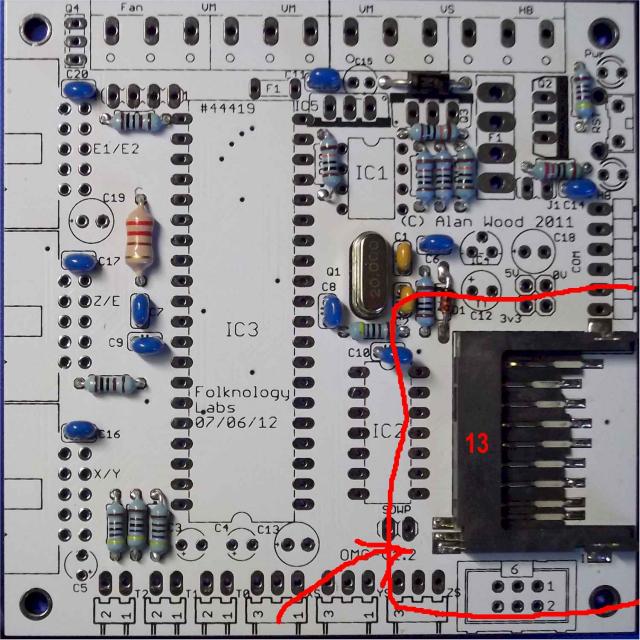
Fit the SD Card holder. It has bumps on its underside that should hold it in position through the two holes near the edge of the board. It should bump into position exactly; solder the two outside tabs first and then the inner and outer legs. All soldering is on the top for this surface-mount component.
|
|
Step 14 |
|
|
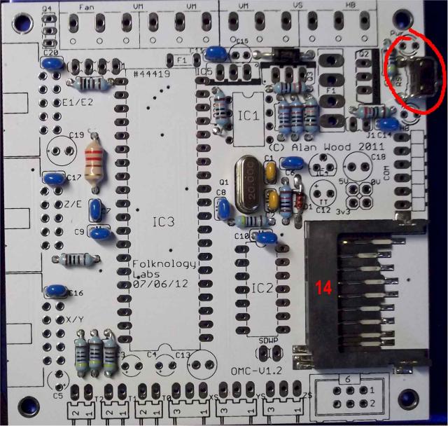
Fit the reset button, facing outward. Solder all four legs, the rear two are supports. |
|
Step 15 |
|
|
The markings on the board may be partially covered by the adjacent below printed line. |
|
Step 16 |
|
|
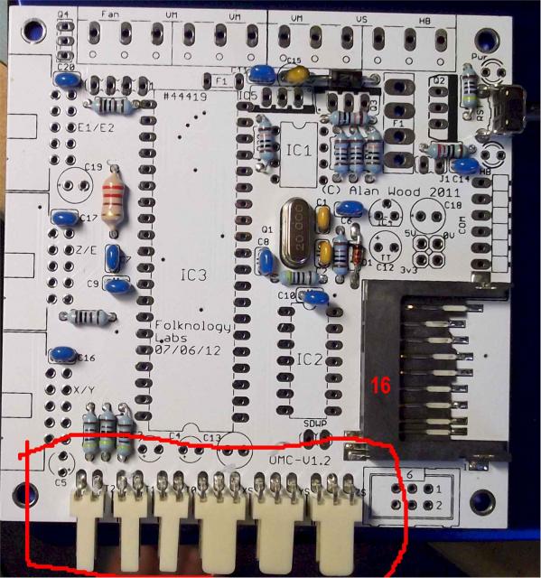
Fit three 2-pin connectors and three 3-pin ones at the bottom of the board. [thermistor (2-pin) and endstop (3-pin) connectors] |
|
Step 17 |
|
|
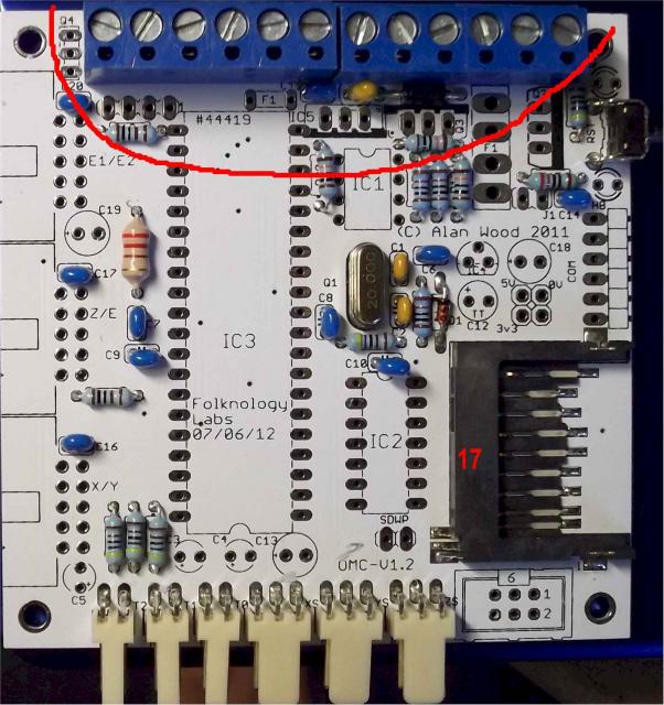
Fit the two six screw terminals at the top of the board. Facing outward. Note that these components may have a notch at one end and a corresponding bump at the other. So they can be assembled into, effectively, a single 12 screw terminal before positioning on the board. If you fit one 6 screw terminal block and solder it into position, you may find it hard to fit the other afterwards. |
|
Step 18 |
|
|
Fit the right-angled black-boxed 10-pin headers on the left side of the board [connections for cables to driver modules]. |

|
Step 19 |
|
|
|
|
Step 20 |
|
|
|
|
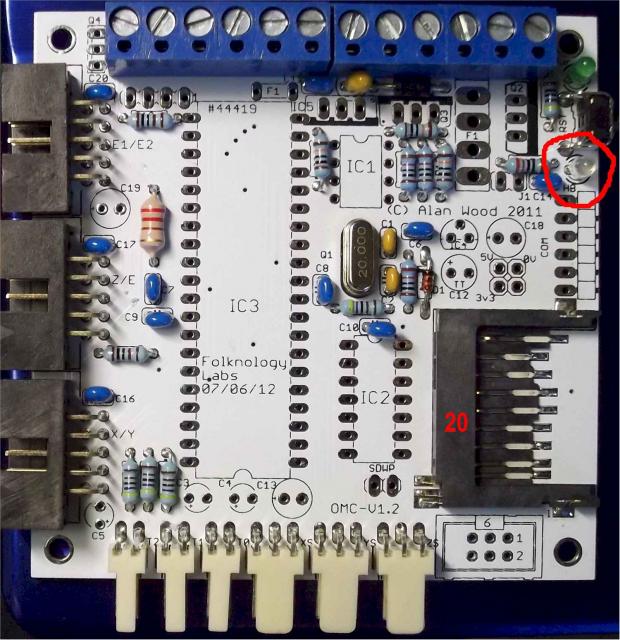
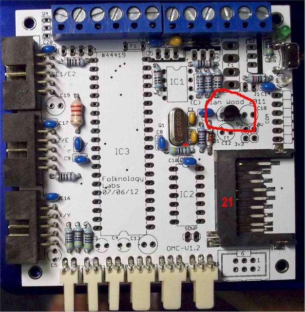
Step 21 |
|
|
Fit the Voltage Regulator IC4 LP2950Z labelled 7CM151E KY5033 (or 'N99AC, 2950A, CZ3.3') at IC4 with the flat face towards the bottom of the board, as shown on the markings on the board. |
|
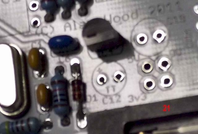
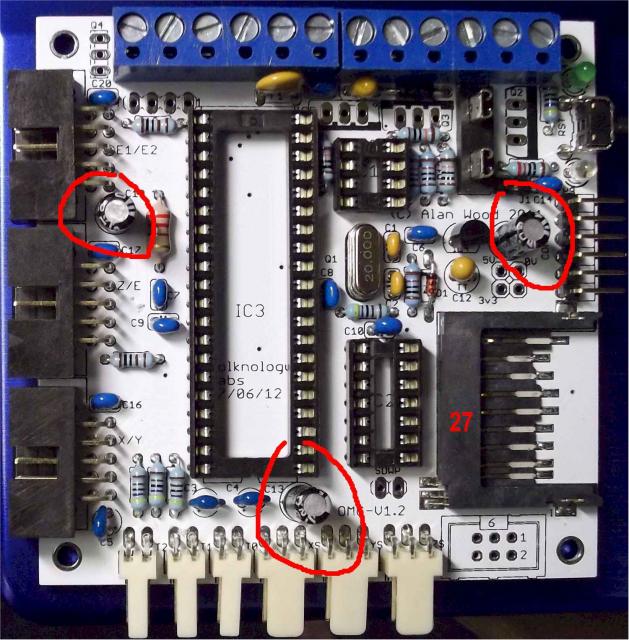
Step 22 |
|
|
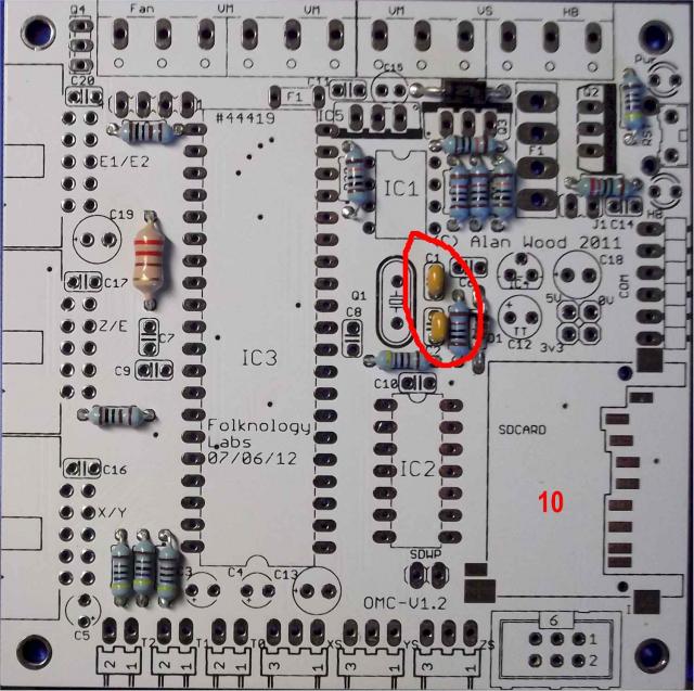
Fit the larger gold-coloured tantalum 22μF capacitor at C12 below IC4 with long leg to + mark on board. Observe the correct polarity (positive to the left). Note that the legs on this need to be carefully squeezed together to avoid putting pressure on the gold body part. NOTE (admg 2014-02-09): For Round 3 a 33μF tantalum capacitor was substituted.
|
|
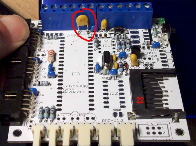
Step 23 |
|
|
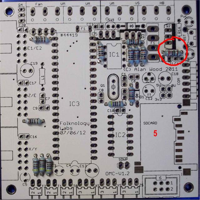
Fit F1 PTC fuse at top of board below terminals above IC3 position. |
|
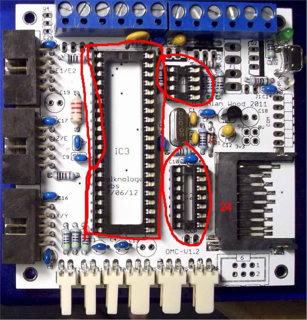
Step 24 |
|
|
Fit the three DIL IC sockets. Your sockets may be marked with a notch or a square hole that aligns with the marking on the board, i.e. at the bottom for the large IC1 and at the top for the two small ones at IC2 and IC3. |
|
Step 25 |
|
|
Fit 3 10uf ceramic blue caps at c3,c4,c5 in bottom left, ignore the polarity marking |

|
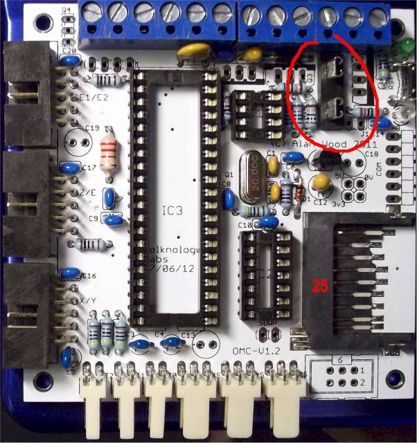
Step 26 |
|
|
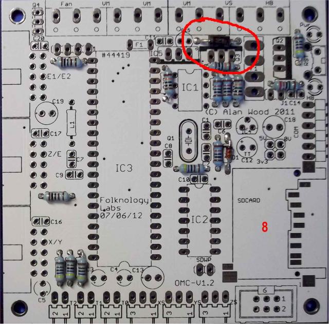
Fit fuse holder F1 (4 pin) top right |
|
Step 26a |
|
|
Fit FTDI header at COM square and level |
|
Step 27 |
|
|
|
|
Step 28 |
|
|
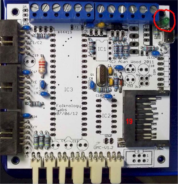
Fit the one 2-pin jumper in the space marked J1 in top right |

|
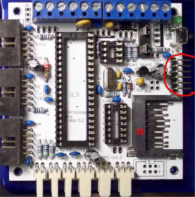
Step 29 |
|
|
Fit the SPI/ISP header at the bottom right. these are just plain pins now. |

|
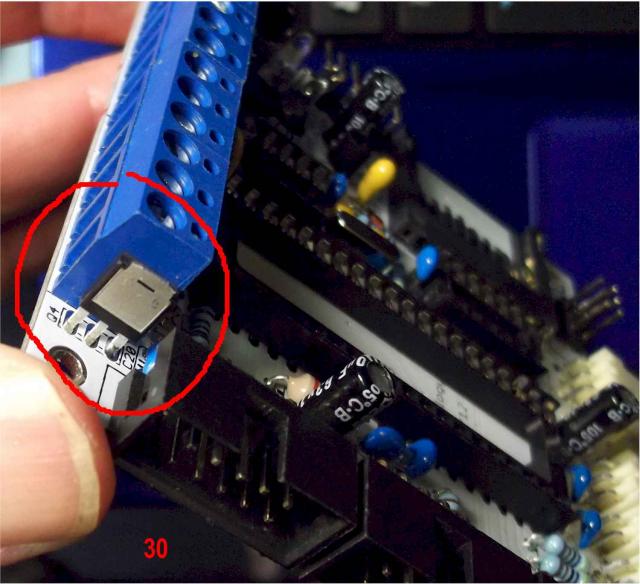
Step 30 |
|
|
|
|
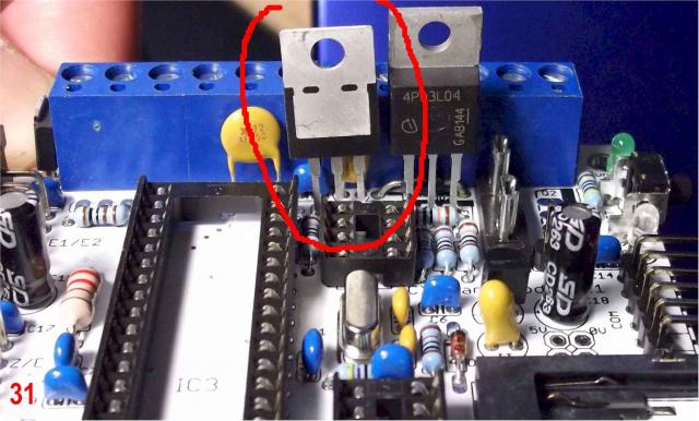
Step 31 |
|
|
|
|
Step 32 |
|
|
|

|
Step 33 |
|
|
|

|
Nearly Complete! |
|
|
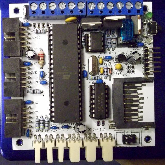
Ensure that all the legs of each chip are in the socket correctly before pressing the chip home. It can happen that a leg misses the socket and gets bent outside. You may wonder about the components that have NOT been fitted:
|
|